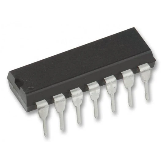
CMOS 8-Input NAND/AND Gate IC - CD4068
CMOS 8-Input NAND/AND Gate IC - CD4068
CD4068 CMOS 8-Input NAND/AND gate IC provides the system designer with direct implementation of the positive logic 8 Input NAND and AND functions and supplements the existing family of CMOS gates.
Specifications:-
- High Voltage Type (20V Rating)
- Medium Speed Operation - TPHL, TPLH = 75ns (Typ.) at VDD = 10V
- Buffered Inputs and Outputs
- 5V, 10V and 15V Parametric Ratings
- Standardized Symmetrical Output Characteristics
- 100% Tested for Quiescent Current at 20V
- Maximum Input Current of 1µA at 18V Over Full Package Temperature Range; 100nA at 18V and +25oC
- Noise Margin (Over Full Package/Temperature Range) - 1V at VDD = 5V - 2V at VDD = 10V - 2.5V at VDD = 15V
Original: $16.00
-70%$16.00
$4.80Description
CMOS 8-Input NAND/AND Gate IC - CD4068
CD4068 CMOS 8-Input NAND/AND gate IC provides the system designer with direct implementation of the positive logic 8 Input NAND and AND functions and supplements the existing family of CMOS gates.
Specifications:-
- High Voltage Type (20V Rating)
- Medium Speed Operation - TPHL, TPLH = 75ns (Typ.) at VDD = 10V
- Buffered Inputs and Outputs
- 5V, 10V and 15V Parametric Ratings
- Standardized Symmetrical Output Characteristics
- 100% Tested for Quiescent Current at 20V
- Maximum Input Current of 1µA at 18V Over Full Package Temperature Range; 100nA at 18V and +25oC
- Noise Margin (Over Full Package/Temperature Range) - 1V at VDD = 5V - 2V at VDD = 10V - 2.5V at VDD = 15V